Task/Objective:
SEM imaging of materials and micro-devices.
Element analysis (mapping).
Specific information on the method:
Resolution SEM: 0.8 nm @ 15 kV, 1.4 nm @ 1 kV
Acceleration Voltage: 0,02 – 30kV
Magnification: 12 – 2,000,000 x in SE mode
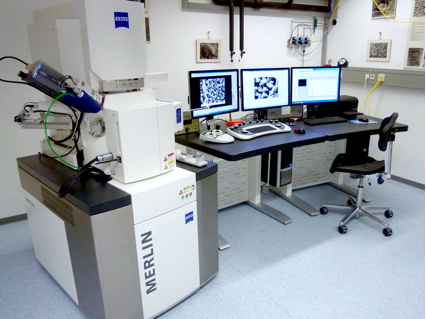
Specific information on the equipment/instrumentation:
Computerized Field Emmission (FE) – Scanning Electron Microscope (SEM) with Patented GEMINI II electromagnetic/electrostatic objective lens system.
Resolution SEM: 0.8 nm @ 15 kV, 1.4 nm @ 1 kV
Acceleration Voltage: 0,02 – 30kV
Magnification: 12 – 2,000,000 x in SE mode
Detectors:
- Chamber Detectors (Everhart-Thornley SE detector)
- In-lens SE Detector (mounted in GEMINI column)
- In-lens Energy-selective-Backscatter (EsB) detector (energy selective detection (grid voltage 0-1500V) of high angle BSEs)
- AsB detector (detection of low angle BSEs)
- EDS-System Bruker QUANTAX EDS-Detector (60mm²).
Other: Gas Injection System (N2) for charge compensation.
Samples/limitations:
Target must be stable under vacuum and should not degas.
A transfer system for air sensitive samples is available.
Examples of typicaly analytical questions:
Studying material or micro device (e.g. battery electrodes) structures. Determination of element distribution.
Fields of research:
Primarily, materials for programs to Renewable energy and its energy storage facilities (e.g. Lithium batteries).